Wafer Probing

Wafer Probing is used after the integrated circuits are applied to the wafers. To do this, the wafers are mounted on an xy-unit and connect to the contact pads (connection pads) with very thin pins. Since the test equipment connected to these pins only provides the individual chips with a voltage, it tests the correct functioning of each individual chip at the same time. The function test in the front-end process can fail in a more significant and intensive way than at a later point in time if only non-contact inspection is possible.

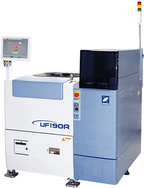
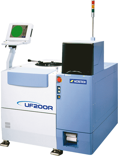
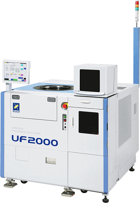
≤ 200 mm Wafer Prober

The right solution for every requirement: from proven, fully automatic basic models to ultra-quick high end models with the highest precision in a large temperature range.

UF190R
 UF200R
 UF2000

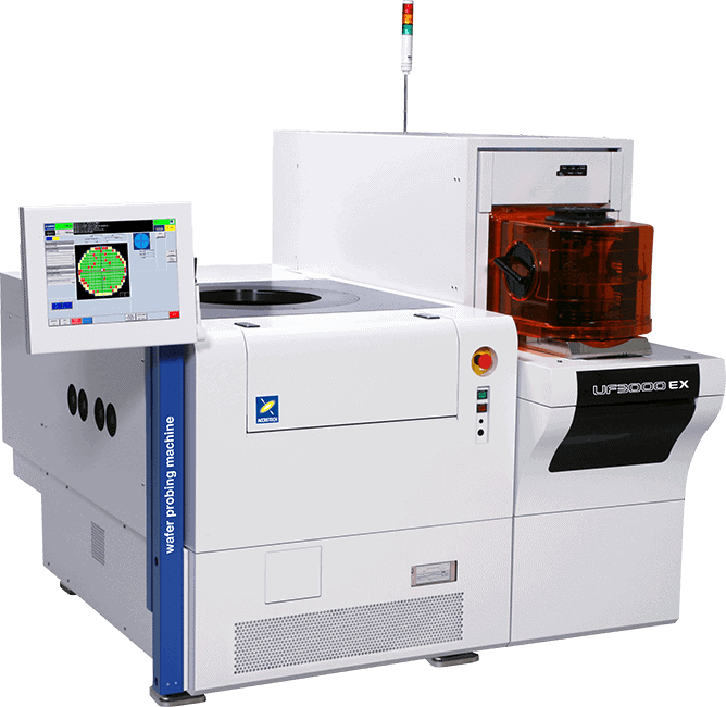
≤ 300 mm Wafer Prober

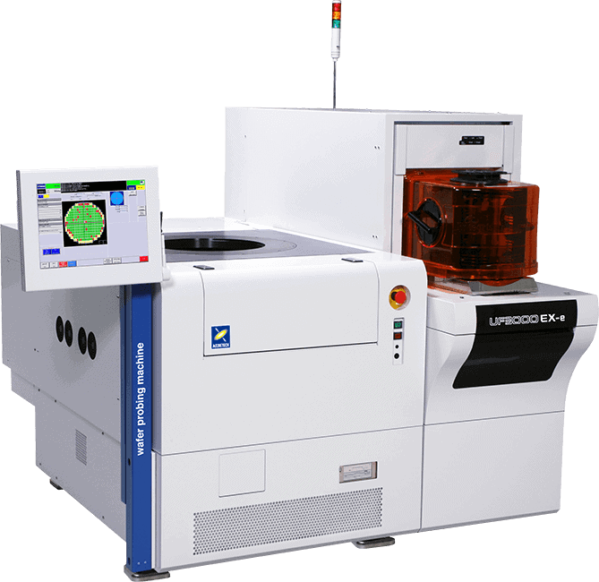
High throughput and +-1.5 µm precision for wafers up to 300 mm diameter. Can be adapted to all testing environments and make simple handling and navigation possible.

UF3000EX
 UF3000EX-e

Wafer and Frame Probers

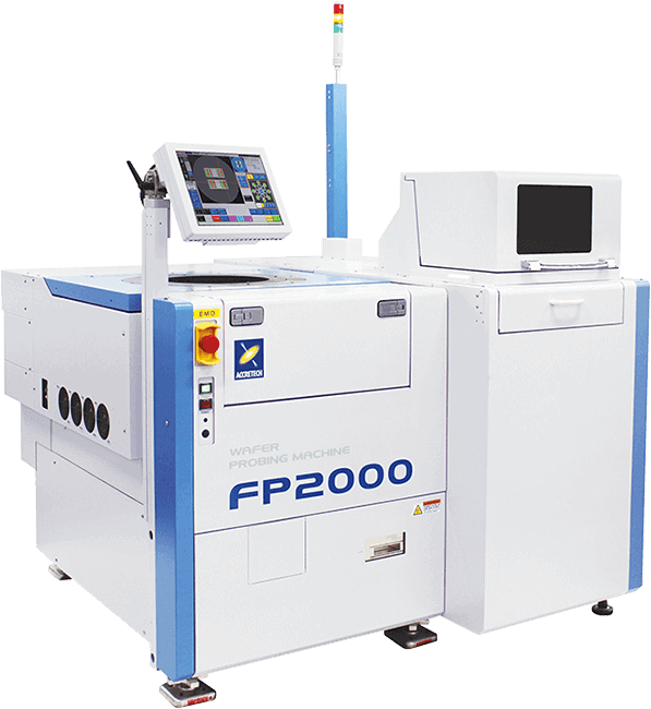
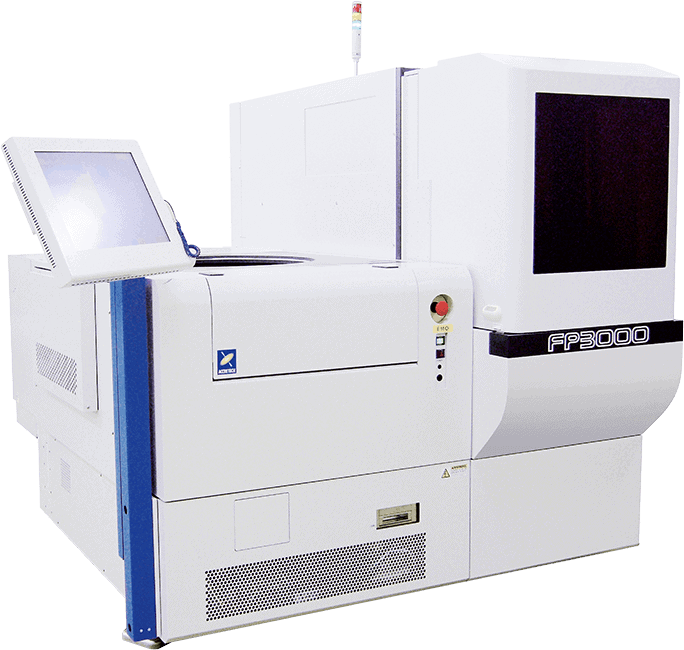
Great flexibility. The Frame Handling Probers can be used for both testing ultra-thin wafers and for wafers on a dicing frame.

 FP2000
 FP3000

Key Features

High Voltage

High Current

Vacuum-less handling (MEMS)

Light-free 

Group Index

Bump Probing

Color Camera

Super-high Magnification camera

Mini environment (ISO xx)

OHT

Thin Wafer

Ultra Thin Wafer

Top-side handling

We are here for you.

+49 (0) 89 546788-0

contact us